
Silicon Photonics.
Perfectly Aligned.
Innovative e-MEMS improving precision, stability and speed of optical alignment. Enhancing efficiency. Unlocking volume production.
e-MEMS also powering: 6G RF Nanosensors AIoT
Silicon Photonics.
Perfectly Aligned.
Innovative e-MEMS improving precision, stability and speed of optical alignment. Enhancing efficiency. Unlocking volume production.
e-MEMS also powering: 6G RF Nanosensors AIoT
Creative Nanodevices
The next revolution in semiconductors and silicon photonics
Nanusens has developed a breakthrough embedded MEMS technology that builds nanoscale structures within the layers of a standard CMOS chip.

Nanosensors
Our e-MEMS Sensors are so small they are actually nanosensors. Many different sensors can be built into the same tiny chip to add extra functionality and there is more space to include larger batteries for longer operational life.

Tunable Capacitors
Our e-MEMS Tunable Capacitors (TCs) can be integrated within the CMOS layers to form an ultra-compact single chip solution for the RF front end of 6G mobile phones. These TCs can deliver higher antenna efficiency and 90% longer talk times.

Actuators
Our e-MEMS Actuators help address key challenges with silicon photonics, such as optical misalignment and MRR thermal detuning. Our novel technology means that nano-mechanical devices can be incorporated inside silicon photonic chips.
Understanding MEMS
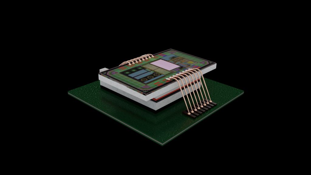
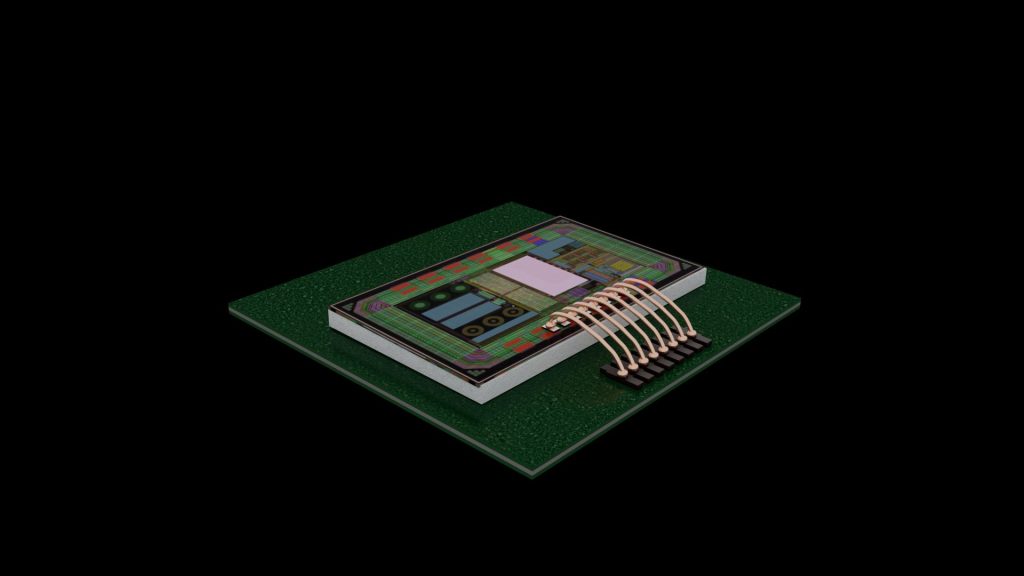
Put simply – MEMS is when there are integrated circuits or chips with nano-mechanical devices inside. MEMS (Micro Electro-Mechanical Systems) is needed for the next generation of sensors, RF solutions, silicon photonics and AI systems. But traditional MEMS involves bespoke processes and production on custom lines by specialized companies. This makes it very expensive and difficult to scale up.
Embedded MEMS in CMOS
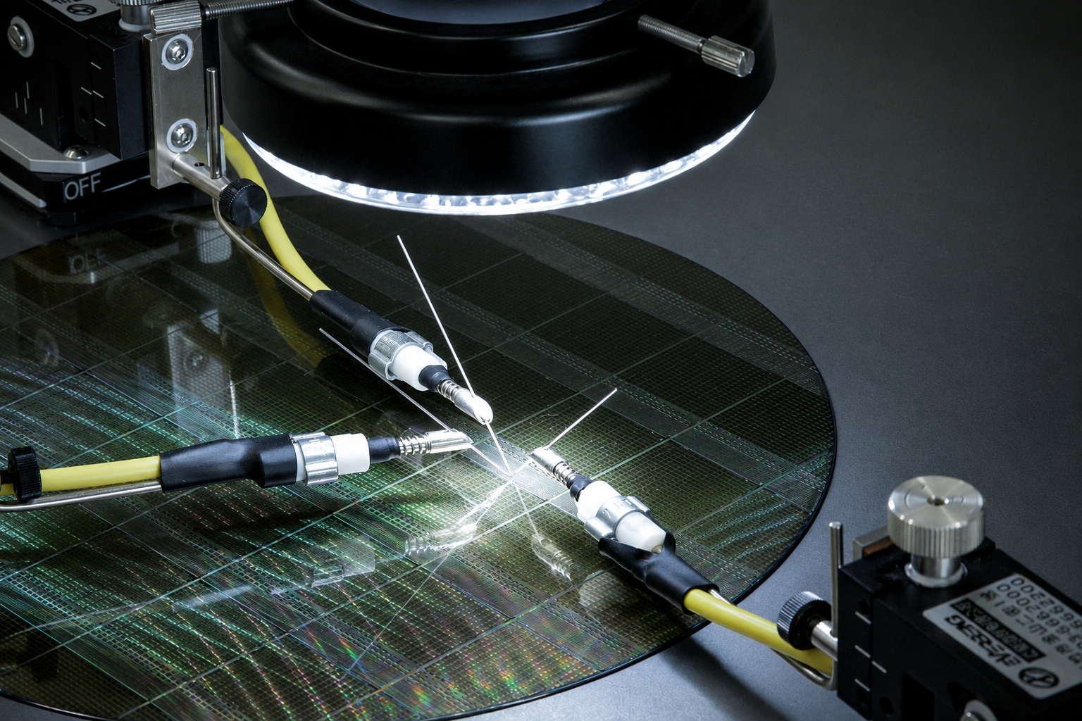
Embedded MEMS in CMOS
CMOS is the standard manufacturing process for solid state chips. Our innovative e-MEMS is created using the standard CMOS process, allowing for high volume production and radically reducing costs. The resulting e-MEMS and the required control circuitry form single chip solutions that are significantly smaller than multi-component equivalents, and offer enhanced performance and energy efficiency.
NANO-MECHANICAL DEVICES
The only company with NEMS-within-CMOS
We have invested over fifteen years and more than €14 million in Research and Development to perfect our unique approach of building NEMS (Nano Electro Mechanical Systems) structures within the CMOS layers. We are protecting these designs with comprehensive patents to secure our position as the only company with NEMS-within-CMOS.

Ultra small
Our nanoscale sensor structures are up to ten times smaller.
Current MEMS structures have feature sizes of one micron or larger while our NEMS (Nano Electro Mechanical Systems) structures
have features of 0.3 microns or less. This is a 100x area reduction.

Save space
A typical MEMS sensor package needs two chips - one for the MEMS structure and another for the control electronics, resulting in a package of 4mm3. As our NEMS sensor package has everything on one chip we can reduce the size by orders of magnitude.

Multi-sensor solutions
Additional NEMS sensor structures can be added to the same chip with hardly any increase in size. These sensor structures would be similar in size and most of the control electronics is shared. This means that a multi-sensor solution is only slightly larger.

Unlimited production volumes
Our disruptive technology will revolutionize the semiconductor and silicon photonics sectors by removing the barrier to high volume production. We can use any CMOS fab and enjoy the cost-saving benefits of CMOS shrinking to smaller nodes.
Applications
Our e-MEMS technology enables breakthroughs across three key application areas: Silicon Photonics, 6G RF and AIoT.
Applications
Silicon Photonics
Our solution for optical misalignment and MRR thermal detuning.
Misalignment is a significant challenge. Our nano-aligner reduces laser alignment time from several minutes to only a few seconds. There is also a locking mechanism after alignment to ensure accuracy and stability, with the option to realign at any point if needed. This enables volume production.
Our unique solution is ultra-small size, low-cost, high-performance and energy-efficient. With our MRR thermal detuning, power consumption is minimal and the mechanical frequency/speed response is much faster.
Applications
6G RF Front End
Our solution for the RF challenges of next-generation mobile phones.
The 5G RF front end needs to be redesigned for the challenges of many more and higher frequencies required by 6G mobile phones. Thanks to our e-MEMS Tunable Capacitors (TCs), we are the only company with an antenna tuning solution that meets the needs of the RF front end of 6G mobile phones.
Our nanoscale capacitors are embedded into the same chip as the control circuitry to give a much smaller, single chip solution than the SOI approach of discrete components on a PCB and with much better performance.
Applications
AIoT
Our sensors as IP solution for next-generation smart devices.
We have a cutting-edge technology that slashes the costs and size of sensors to almost nothing and means that sensor data can be gathered in a completely new way, accelerating AIoT. We can provide our e-MEMS Sensors as IP to integrate directly into ASIC floor plans using standard EDA tools.
Smart devices can be made smarter by adding more sensors with virtually no cost or size penalty. It’s now possible to create ultra-small, low-cost, multi-sensor IoT devices to gather masses of data for next generation AI.
Analysts quotes about Nanusens
Latest Media Coverage
Why Innovation in MEMS technology is impacting the future of mobile phones
June 22, 2026

Why new developments in MEMS are fundamental for next-generation devices
May 5, 2026

The crucial part sensors and MEMS play in smart wearables
January 20, 2026

Creating On-Chip MEMS Sensors in CMOS
December 9, 2025
Electronic Specifier’s top podcasts of 2025
December 3, 2025

Want Nano-Scale, CMOS-Based MEMS Sensors?
November 18, 2025